Seed II Funding in Progress

3D Chips
with 2D Materials

Ease on Three-dimensional Memory & Logic Solutions. FS2 pioneers atomic-scale 2D semiconductor technology for low energy-consumption, cost, and latency computing.

Absolute
Cost Efficiency Maximized
Maximize
Energy Saving Potential
Low-Temp
Process
Wafer Scale
Industrial compatible

The Post-Silicon Era Starts Here

The faster compute, more energy dilemma. AI needs efficiency—global data center power consumption will reach 945 TWh by 2030. Silicon alone cannot keep up beyond 2030.
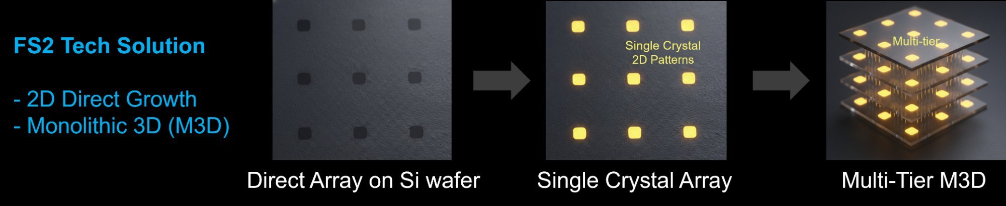
FS2 develops "atomic" 2D semiconductors (2D Materials) that enable monolithic 3D integration at low temperature—compatible with legacy IC infrastructure.

Single Crystal 2D on Any Surface
Wafer-Scale Process
Plug-and-Play with Si Fabs
Multi-Tier M3D Integration
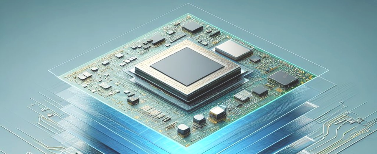
M3D Chip Architecture
01

2D Material Layer

Wafer-scale 2D Materials growth

02

Monolithic Integration

3D sequential integration technology

03

Low-Temp Process

Thermal budget management for BEOL

Core Tech
Atomic-layer MOCVD Growth
IP Portfolio
Multiple 3D Stacking Patents

AI Is Hitting a Wall.
We're Breaking Through It.

As AI models grow exponentially, the gap between compute speed and memory bandwidth widens every year. This is the Memory Wall — and it's becoming the defining bottleneck of the AI era.

The Bottleneck

AI models are scaling 240× every two years.
Memory bandwidth is not keeping up.

FS2's Answer

Stack memory directly on logic.
Eliminate the gap entirely.

FS2 is building the technology to break the Memory Wall — enabling the next generation of AI chips that are faster, denser, and radically more efficient.

World's First Single-Crystal 2D on Amorphous Films

Breaking the thermal barrier with low-temperature growth ready for monolithic integration.

01

2D Material Layer

Wafer-scale 2D Materials growth

02

Monolithic Integration

3D sequential integration technology

03

Low-Temp Process

Thermal budget management for BEOL

Exceptional
Thermal Stability & Reliability
Maximum
Energy Efficiency for AI Workloads
Superior
Carrier Mobility & Transconductance

The Right Team for the Hardest Problems

World-class experts in 2D materials, semiconductor physics, and deep-tech commercialization.

Jekyung Kim
Leadership

Jekyung Kim

Co-CEO & Co-Founder

Sang-Hoon Bae
Leadership

Sang-Hoon Bae

Co-CEO & Co-Founder

Intak Jeon
Operations

Intak Jeon

COO

Chankeun Park
Research

Chankeun Park

Director of R&D

Bo-In Park
Engineering

Bo-In Park

Director of Engineering

Yeji Park
Process Engineering

Yeji Park

Process Engineer

Hyeonuk Jung
Process Engineering

Hyeonuk Jung

Process Engineer

Advisory Board
Sungkyu Lim
Advisory Board

Sungkyu Lim

Advisor

Jeehwan Kim
Advisory Board

Jeehwan Kim

Advisor

Kyusang Lee
Advisory Board

Kyusang Lee

Advisor

Build the Future with Us

For those daring to innovate. Join us in pioneering the next generation of semiconductor technology.

💼

Investment

Seed II funding
in progress

🤝

Partnership

Equipment & process
innovation

👥

Careers

Join world-class
experts

[email protected]